Impact of nanoscale morphology on charge carrier delocalization and mobility in an organic semiconductor
https://onlinelibrary.wiley.com/doi/10.1002/adma.202104852
Electronic devices made of flexible organic materials have revolutionized the semiconductor industry in this century. Yet, their performance is often limited by the relatively modest charge mobility of these materials, usually attributed to structural defects and disorder. How charge carriers propagate through disordered organic semiconductors, transition between amorphous and crystalline domains and navigate across grain boundaries remains largely unknown so far.
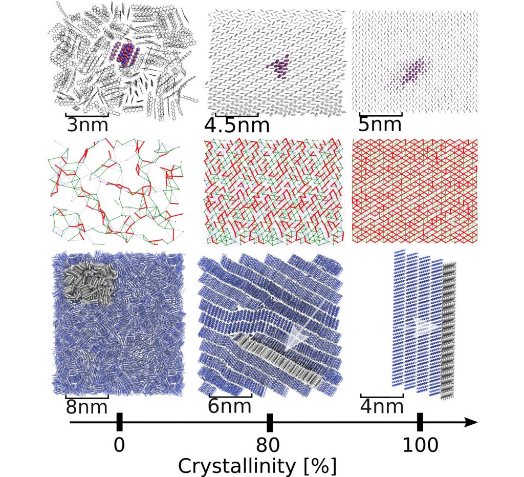
In this paper PhD student Matt Ellis and co-workers from Jochen Blumberger’s group present a computational methodology that fills this gap and apply it to a prototypical molecular organic semiconductor, pentacene. Jochen’s group found that charge carriers are more delocalized, that is, more “quantum” than previously thought, even for relatively disordered samples, and they establish the mechanism of charge transport as a function of crystallinity.
The methodology is generally applicable to any molecular organic semiconductor and may be used in future work for identifying new disordered materials with high charge mobility.
M. Ellis, H. Yang, S. Giannini, O. G. Ziogos, and J. Blumberger